Computers work according to basic principles at various levels. Low level, how the hardware actually works. Principles guiding operating system resource management and interactions with hardware and application software.
By the end of this lesson, you will be able to:
Explain the role of the CPU and its main components
Describe how the control unit, ALU, and registers work together
Understand the function of buses and their types
Compare single-core and multi-core processors
Apply knowledge to real-world computing scenarios
The Central Processing Unit (CPU) functions as the brain of a computer system, responsible for executing instructions that comprise computer programs. It performs arithmetic, logical, control, and input/output operations.
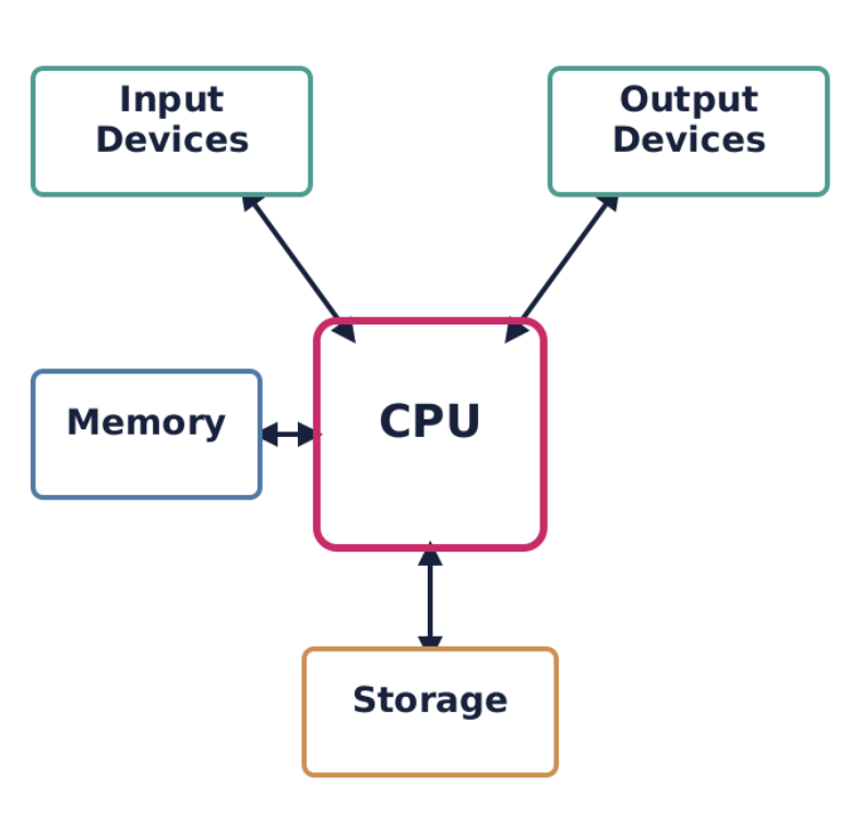
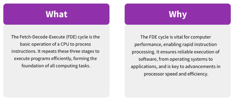
The CPU’s primary role is to process data by carrying out instructions. These instructions are fundamental operations like adding two numbers, moving data from one location to another, or making a decision based on a comparison. Every action a computer takes, from opening an application to displaying an image, ultimately breaks down into a series of instructions that the CPU executes.
For instance, when a user clicks an icon to launch a web browser, the operating system translates that click into a series of instructions. These instructions might include:
Loading the browser’s program code from storage (e.g., SSD) into main memory (RAM).
Allocating memory space for the browser process.
Initializing various browser components.
Beginning to fetch instructions for rendering the browser window.
Another example occurs when a user types a character on the keyboard. The CPU receives an interrupt signal indicating keyboard input. It then executes instructions to:
Read the scan code from the keyboard controller.
Translate the scan code into a character (e.g., ASCII or Unicode).
Store the character in a buffer.
Display the character on the screen by sending instructions to the graphics card.
A hypothetical scenario might involve a simple embedded system controlling a smart thermostat. When the thermostat detects the room temperature has dropped below a set point, the CPU executes instructions to:
Read the current temperature sensor value.
Compare it to the desired temperature set point.
If below the set point, send a command to the heating system to turn on.
Continuously monitor the temperature until it reaches the set point, then send a command to turn the heating off.
Real-World Application
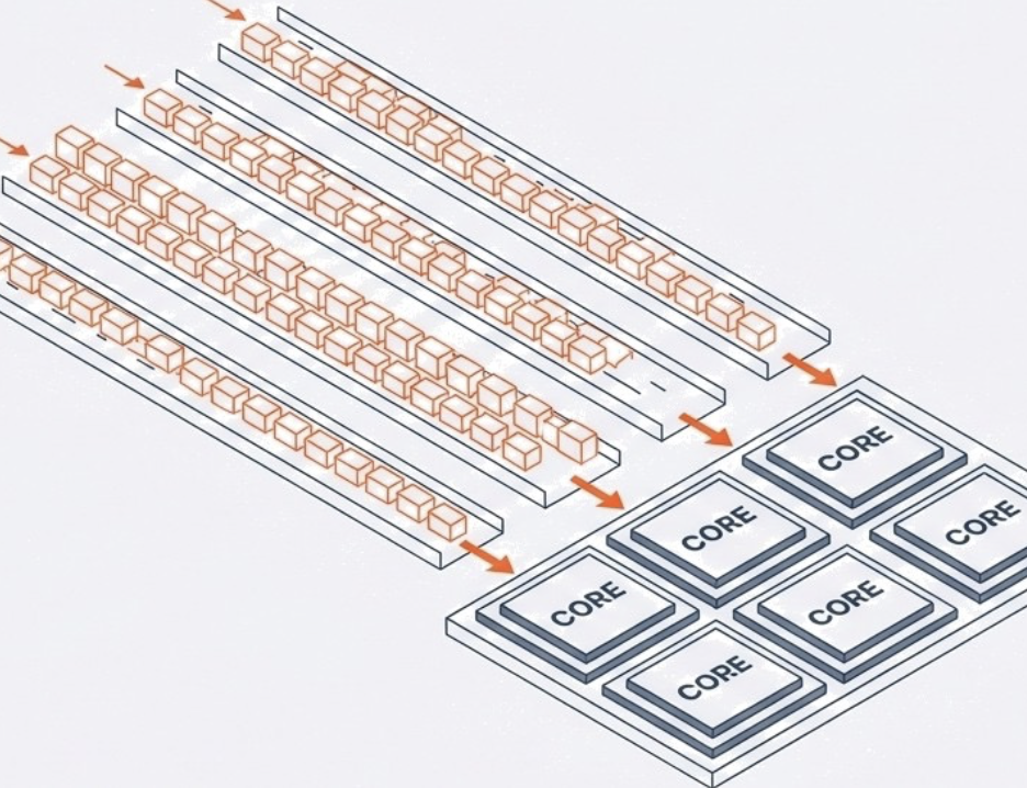
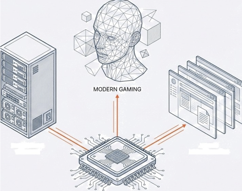
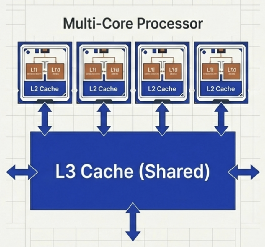
Modern CPUs are incredibly complex, but their high-level function remains consistent across various applications. In data centers, massive server CPUs manage millions of transactions per second for online services. Each transaction involves fetching instructions for database queries, processing data, and often sending results across a network. Similarly, in your smartphone, a low-power CPU manages background apps, processes touch inputs, and orchestrates communication with cellular and Wi-Fi radios. The core principle of fetching instructions, processing data, and interacting with other components holds, regardless of scale or specific application. The efficiency and speed of these high-level interactions are paramount for overall system performance, whether in a supercomputer or a tiny embedded device.
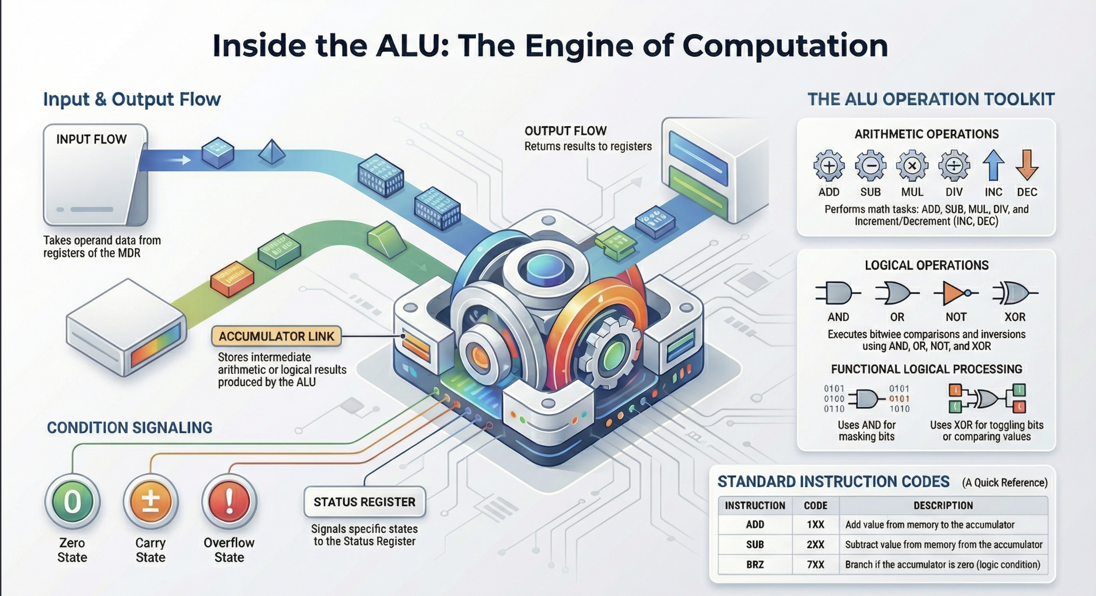
While the CPU is central, it does not operate in isolation. It constantly interacts with other crucial components of a computer system to perform its tasks. These interactions primarily occur through various communication pathways known as buses.
Main memory, or Random Access Memory (RAM), is where the CPU temporarily stores the instructions of active programs and the data these programs operate on. The CPU constantly fetches instructions from RAM to execute them and writes results back to RAM. This interaction is critical because the CPU’s internal storage (registers) is very limited, and persistent storage (like SSDs) is too slow for direct, continuous instruction fetching.
Consider a video editing application. When you load a large video file:
The CPU instructs the storage controller to transfer segments of the video file from the SSD into RAM.
As you apply effects or cut scenes, the CPU fetches instructions from the video editor program (also in RAM) and processes sections of the video data (from RAM), storing temporary results back into RAM.
Only when you explicitly save the project are these changes written back to the SSD.
I/O devices, such as keyboards, mice, monitors, printers, and network cards, allow the computer to interact with the external world. The CPU manages all communication with these devices. When you move your mouse, the mouse sends signals to the CPU via a controller. The CPU processes these signals and translates them into cursor movement on the screen. Similarly, when the CPU needs to display graphics, it sends data and commands to the Graphics Processing Unit (GPU), which is itself a specialized I/O device designed for rendering.
A practical example is printing a document:
The CPU sends the document data and print commands to the printer controller.
The printer controller buffers the data and manages the physical printing process.
The CPU may periodically check the printer’s status (e.g., paper jam, ink level) by querying the controller.
Storage devices like Hard Disk Drives (HDDs) and Solid State Drives (SSDs) provide long-term, non-volatile storage for data and programs. The CPU initiates read and write operations to these devices when programs need to be loaded, files need to be saved, or data needs to be accessed that is not currently in RAM. The CPU communicates with storage devices through dedicated controllers.
When installing a new software application:
The CPU directs the storage controller to read the application’s installation files from the installation media (e.g., download cache, USB drive).
It then processes these files, writes them to the designated installation directory on the SSD, and possibly updates system registries, all through coordinated commands to the storage controller.
The CPU is made up of two main units: the control unit (CU) and the arithmetic logic unit (ALU).
The Control Unit acts as the CPU’s orchestra conductor, directing operations without performing them.
Core Functions:
Directs Data Flow: Manages data movement between CPU, memory, and I/O devices.
Instruction Cycle: Orchestrates the Fetch-Decode-Execute cycle, guiding the ALU.
Timing: Utilizes a system clock for precise operation sequencing and synchronization.
How the CU Works in a Nutshell:
The Control Unit is often considered the “brain within the brain” of the CPU. It is responsible for orchestrating the CPU’s entire operation, directing the flow of data, and managing instruction execution. It interprets instructions and generates control signals that tell other components (like the ALU, registers, and buses) what to do and when to do it.
The control unit is in constant communication with all other parts of the CPU.
It reads the IR to know what to do.
It sends control signals to registers to load or store data.
It signals the ALU to perform specific operations.
It controls the MAR, MDR, and the system buses for memory access.
It updates the PC for instruction sequencing or jumps.
Consider a LOAD R1, [Address] instruction.
The LOAD R1, [Address] instruction is fetched into the IR.
The CU decodes this instruction, recognizing it as a memory read operation.
The CU extracts the Address operand and sends it to the MAR.
The CU then activates the control signals on the system bus to initiate a memory read.
Data from Address is read from memory and placed into the MDR.
The CU then generates control signals to move the data from the MDR into R1.
Finally, the CU increments the PC to point to the next instruction.
The ALU is the musician of the CU’s orchestra, performing all actual processing.
Core Functions
Arithmetic: Handles all mathematical calculations (add, subtract, multiply, divide).
Logic: Makes logical comparisons (AND, OR, NOT, XOR) for true/false outcomes.
Decision Making: Enables program branching through number comparisons.
It is a fundamental component for all data manipulation within the CPU.
The ALU takes input data (operands) from registers or the MDR, performs the requested operation, and then typically places the result back into a register or the MDR. It also signals conditions (like zero, carry, or overflow) to the Status Register.
Arithmetic Operations:
Addition: ADD
Subtraction: SUB
Multiplication: MUL
Division: DIV
Increment/Decrement: INC, DEC
Logical Operations:
AND: Performs a bitwise AND operation. Often used for masking bits (e.g., clearing specific bits).
OR: Performs a bitwise OR operation. Often used for setting specific bits.
NOT: Performs a bitwise NOT (inversion) operation.
XOR: Performs a bitwise exclusive OR operation. Often used for toggling bits or comparing values (XORing a value with itself results in zero).

Shift Operations:
Logical Shift Left/Right: Shifts bits to the left or right, filling vacated positions with zeros. Used for efficient multiplication or division by powers of 2.
Arithmetic Shift Right: Shifts bits to the right, preserving the sign bit. Used for signed integer division by powers of 2.
Rotate Left/Right: Shifts bits, but bits that “fall off” one end are inserted at the other end.
Comparison Operations:
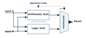
CMP: Compares two operands by performing an internal subtraction and updating the flags register, but without storing the result. This allows subsequent conditional jump instructions to make decisions based on the comparison (e.g., JG—Jump if Greater).
Operands flow from registers or memory (via MDR) into the ALU. The Control Unit directs the ALU to perform a specific operation based on the decoded instruction. The result of the operation is then typically written back to a destination register.
Real-world Example 1: ADD R1, R2
The values from R1 and R2 are sent to the ALU’s input operands.
The Control Unit signals the ALU to perform an addition.
The ALU performs R1 + R2.
The result is sent back to R1 (or another designated destination register).
The ALU also updates the flags in the Status Register based on the result (e.g., if the sum is zero, the Zero Flag is set).
Registers are small, high-speed storage locations within the CPU itself, used to hold data, instructions, and memory addresses that the CPU is actively working with. Think of them as the CPU’s ‘working hands’ holding tools while a job is being done. Unlike main memory (RAM), which is external to the CPU, registers offer almost instantaneous access, making them critical for the CPU’s performance. The CPU relies on registers to quickly access operands, store intermediate results, and manage program control.
Registers can be broadly categorized into two main types: general-purpose registers and special-purpose registers. Modern CPUs often have a large number of registers, typically 32 or 64 in 64-bit architectures, like those found in x86-64 or ARM processors.
Common Types and Functions (x86 Architecture)
Accumulator Register (AX, EAX, RAX): Primarily used for arithmetic operations, logical operations, and storing function return values.
Base Register (BX, EBX, RBX): Used to hold the base address of memory for accessing data.
Counter Register (CX, ECX, RCX): Primarily used as a counter for string and loop operations.
Data Register (DX, EDX, RDX): Used in multiplication/division operations and I/O port addressing.
Index Registers (SI, DI, ESI, EDI, RSI, RDI): Used for string operations and indexing in memory.
Stack Pointer (SP, ESP, RSP): Manages the stack top.
Base Pointer (BP, EBP, RBP): Points to the base of the stack frame.
Extended 64-bit Registers (R8-R15)
Modern x86-64 architectures include eight additional general-purpose registers (R8 through R15), which can be accessed as 64-bit, 32-bit, 16-bit, or 8-bit, providing more flexibility for complex calculations.
General Classification
Beyond specific names, GPRs are often classified by their function:
Data Registers: Used for arithmetic/logical operations (e.g., AX, BX, CX, DX).
Pointer Registers: Used for memory addressing (e.g., SP, BP).
Index Registers: Used for string and array operations (e.g., SI, DI).
SPRs have dedicated functions within the CPU and are typically not directly accessible by programmers in the same way GPRs are, although some may be implicitly used by instructions. They are crucial for managing the instruction cycle, memory access, and CPU status.
Program Counter (PC) / Instruction Pointer (IP): This register holds the memory address of the next instruction to be fetched. After an instruction is fetched, the PC is typically incremented to point to the subsequent instruction.
Real-world Example: When you launch a program, the operating system loads the program into memory and sets the PC to the memory address of the program’s entry point. The CPU then begins fetching instructions from that address.
Instruction Register (IR): After an instruction is fetched from memory, it is loaded into the IR. The Control Unit then decodes the instruction stored in the IR to determine what operation needs to be performed.
Real-world Example: If the CPU fetches an instruction like ADD R1, R2, this binary instruction code is placed in the IR. The Control Unit then examines this code to understand it’s an “ADD” operation and that it involves registers R1 and R2.
Memory Address Register (MAR): This register holds the memory address of the data or instruction that the CPU wants to read from or write to main memory.
Real-world Example: If the CPU needs to load a value from memory location 0x1000, it places 0x1000 into the MAR. The memory controller then uses this address to locate the data.
Memory Data Register (MDR) / Memory Buffer Register (MBR): This register temporarily holds the data being read from or written to main memory. When reading from memory, the data retrieved is placed in the MDR before being transferred to a CPU register. When writing to memory, the data to be written is first placed in the MDR.
Real-world Example: Following the previous example, if the CPU reads a value 0xABCD from memory location 0x1000, the 0xABCD value is temporarily stored in the MDR before being moved to a general-purpose register like RAX.
The Accumulator (AC): is a holding area for the Arithmetic Logic Unit (ALU). It stores the intermediate arithmetic or logical results produced during calculation.
Real-world Example: Imagine a simple program adding two numbers.
MOV RAX(AC), 10; Move the value 10 into register RAX(AC)
MOV RBX, 25; Move the value 25 into register RBX
ADD RAX(AC), RBX; Add the content of RBX to RAX (RAX (AC) now holds 35)
Lorem ipsum dolor sit amet, consectetur adipiscing elit. Ut elit tellus, luctus nec ullamcorper mattis, pulvinar dapibus leo.
Discuss! 🤷♀️ 💁♂️ 💬
Critical Thinking
Why are registers necessary if we already have RAM and cache? What would happen to a computer’s speed if the CPU had to access RAM for every single calculation step?
Registers are the CPU’s internal, high-speed storage.
The PC tracks where we are, the IR holds what we are doing, and the MAR/MDR handle communication with memory.
The Accumulator is essential for arithmetic logic.
They are vital because they eliminate the delay of accessing main memory for every single operation.
What is a System Bus?
The Communication Highway
A bus is a critical component that acts like a highway for data. It allows information to travel between the CPU, memory (RAM), storage, and peripherals. This architecture consists of three primary buses: the address bus, the data bus, and the control bus, each playing a distinct role in orchestrating the flow of information. Together, these buses form the crucial pathways that enable the CPU to fetch instructions, process data, and interact with the entire system.
Bus Width Matters
Buses have a width measured in bits (e.g., 32-bit or 64-bit).
Wider bus = More data transmitted at once = Faster performance.
Narrower bus = Less data transmitted at once = Slower performance.
The data bus is a bidirectional pathway used for the actual transfer of data between the CPU, memory, and I/O devices. When the CPU fetches an instruction or reads data from memory, the data travels from memory, over the data bus, to the CPU. Conversely, when the CPU writes data to memory or sends data to an I/O device, the data travels from the CPU, over the data bus, to its destination.
The width of the data bus determines how many bits of data can be transferred simultaneously in a single operation. A wider data bus allows more data to be moved at once, leading to faster overall system performance. For example, a 32-bit data bus can transfer 32 bits (4 bytes) in parallel, while a 64-bit data bus can transfer 64 bits (8 bytes) at a time.
Early 8-bit Systems: CPUs like the Intel 8080 or Zilog Z80 typically had an 8-bit data bus. This meant that memory reads or writes transferred 8 bits (1 byte) at a time. To transfer a larger piece of data, such as a 16-bit word, two separate bus cycles would be required.
Modern Systems: Contemporary desktop and server CPUs typically use a 64-bit data bus, allowing them to transfer 64 bits of data (8 bytes) in a single cycle. This aligns with the CPU’s 64-bit internal architecture and register sizes, enabling efficient movement of large data blocks, which is critical for demanding applications and operating systems. This also directly impacts the performance of memory operations, as more data can be moved to and from RAM simultaneously.
The control bus is a collection of various signals that coordinate and manage the operations of the entire system. These signals are crucial for synchronizing activities, indicating the type of operation (read or write), and handling various states and errors. Unlike the address and data buses, which carry specific information (addresses or data), the control bus carries commands and status signals.
The control bus signals are asserted by the CPU or other bus masters to dictate the operation. For example, to read a byte from memory, the CPU would place the memory address on the address bus, assert the Memory Read signal on the control bus, and then wait for the data to appear on the data bus. The timing and sequence of these signals are critical for proper system operation.
Bidirectional
The control bus sends CPU commands and receives hardware status signals (e.g., ‘Ready,’ ‘Busy’).
The address bus is a unidirectional pathway that the CPU uses to specify the physical location of data or instructions it wants to access in memory or from an I/O device. Each unique location in memory (a byte or a word, depending on the architecture) has a distinct address. When the CPU needs to read from or write to a particular memory location, it places the address of that location onto the address bus. The width of the address bus (i.e., the number of parallel lines it contains) determines the maximum amount of memory the CPU can directly address. For example, an N-bit address bus can address 2^N unique memory locations.
When the CPU wants to access a specific memory location, it asserts the binary representation of that address onto the address lines. Memory controllers or I/O decoders monitor the address bus. When a matching address is detected, the corresponding memory chip or I/O device is activated to prepare for a read or write operation. The address bus does not carry data itself; it only carries the “destination” or “source” information.
Consider a scenario where the CPU needs to fetch an instruction from RAM.
Address Placement: The CPU’s Program Counter (PC) holds the address of the next instruction. The CPU places this address onto the address bus.
Control Signal Assertion: Simultaneously, the CPU asserts the “Memory Read” signal on the control bus, indicating that it intends to read data from the specified memory location.
Memory Response: The memory controller detects the address and the “Memory Read” signal. It then retrieves the instruction (data) from the specified RAM location.
Data Transfer: The retrieved instruction (data) is then placed onto the data bus.
CPU Reception: The CPU reads the instruction from the data bus and transfers it to an internal register, such as the Instruction Register (IR).
This coordinated interplay of the address, data, and control buses ensures that the correct data is accessed from the correct location at the correct time, enabling the CPU to function.
The system bus architecture is not just a theoretical concept; it forms the backbone of all computing systems, from embedded microcontrollers to supercomputers.
Motherboard Design and Chipsets: Modern motherboards feature complex bus architectures, with chipsets (like Intel’s Platform Controller Hub or AMD’s Fusion Controller Hub) acting as sophisticated traffic cops, managing the flow of data across various buses. The traditional “Northbridge” and “Southbridge” architecture has evolved, but the fundamental roles of address, data, and control persist. For instance, the high-speed bus connecting the CPU to the main memory (RAM) is often called the “Front Side Bus” (FSB) or, more recently, integrated directly into the CPU itself (like with Intel’s Integrated Memory Controller or AMD’s Infinity Fabric), but it still segregates address, data, and control signals, even if physically integrated. When you buy RAM, its speed (e.g., DDR4-3200) directly relates to how quickly data can travel across the data bus and the synchronization provided by the control bus.
PCI Express (PCIe): PCIe is a modern high-speed serial bus used for connecting peripherals like graphics cards, NVMe SSDs, and network cards to the CPU. While it’s a serial bus (data bits are sent one after another on each lane) rather than a parallel bus like the older PCI, it still logically implements the address, data, and control functions. For example, when a GPU fetches textures from system RAM, it uses DMA (Direct Memory Access, a concept we will explore later) to initiate memory reads. The GPU effectively becomes a temporary “bus master,” placing addresses on a logical address channel, requesting data via control signals, and receiving data over the logical data channel within the PCIe link. The “lanes” of PCIe (e.g., x16 for a GPU) dictate the aggregate data bandwidth, analogous to the width of a traditional parallel data bus. A PCIe 4.0 x16 slot offers significantly more data bandwidth than a PCIe 3.0 x16 slot, directly impacting how quickly data can move between the GPU and other system components.
Buses are the pathways that connect the CPU, memory, and peripherals.
The Data Bus carries actual information and is bidirectional.
The Address Bus carries location addresses and is unidirectional.
The Control Bus carries commands and timing signals and is bidirectional.
Bus width is crucial: wider buses allow more data transfer and higher memory capacity.
Historically, CPUs had only one core. This meant they could only handle one main task or instruction stream at a time. To improve performance, engineers initially focused on increasing the clock speed (how many operations a core can perform per second). However, physical limitations like heat generation and power consumption made indefinite clock speed increases impractical.
This led to the innovation of multi-core processors. Instead of making one core faster and faster, the industry shifted to integrating multiple independent cores onto a single CPU chip. This marked a significant paradigm shift, allowing computers to process multiple tasks simultaneously, vastly improving efficiency and responsiveness.
At its most fundamental level, a core is the part of the CPU that reads and executes program instructions. Each core contains all the necessary components to perform computational tasks independently
Single-core processors: The linear worker.
Multi-core processors: The parallel array.
Co-processors: The specialist support.
A single-core processor contains exactly one processing unit. This architecture defines the baseline of computing: linear execution. It can strictly handle only one task at a time.
Context: Predominantly found in older machines or low-end computers where cost outweighs performance.
Ideal Workload: Adequate for simple tasks devoid of heavy multitasking. While it can run multiple apps, the CPU must time-share, slowing performance due to frequent switching.
The Functional Illusion: Rapid switching between apps creates the appearance of simultaneous processing.
The Reality: The single CPU is shared. As application volume increases, the CPU’s attention is divided, creating a performance bottleneck.
attis, pulvinar dapibus leo.
A Multi-core processor integrates two or more independent cores onto a single chip. Unlike the illusion of multitasking on a single core, these execute multiple instructions simultaneously.
Dual-core (2)
Quad-core (4)
Hexa-core (6)
Octa-core (8)
By executing instructions in parallel, performance scales to meet the demands of modern, intensive workloads.
Hardware architecture guarantees potential, not speed. Software must be explicitly written to utilise it. Older software or unoptimized software runs at single-core speed, even on multi-core hardware.
A co-processor is a processor built with a distinct purpose. It exists solely to support the main CPU.
The Strategy: Offloading. Complex, specific tasks are removed from the general CPU’s queue and handed to a specialist.
This adds the benefit of parallel execution of highly complex functions (e.g., floating-point arithmetic, graphics, and signal processing).
Core vs. CPU
It is important to distinguish between a “core” and a “CPU.” A CPU is the entire physical chip that plugs into your motherboard. A modern CPU contains one or more cores. So, when you hear about a “quad-core CPU,” it means the single CPU chip has four independent processing units (cores) within it.
The concept of threads is closely related to cores. A thread is the smallest sequence of programmed instructions that can be managed independently by a scheduler, which is typically a part of the operating system.
A single core can execute one thread at a time.
Many modern CPUs feature Hyper-Threading (Intel) or Simultaneous Multi-threading (SMT) (AMD). This technology allows a single physical core to appear as two logical cores to the operating system, enabling it to execute two threads concurrently. While not as powerful as two physical cores, it can improve efficiency by utilizing core resources that would otherwise be idle during certain operations. For instance, if one part of a physical core is waiting for data, the other “logical” core can still be processing another thread’s instructions.
So, a 4-core CPU with Hyper-Threading can effectively handle 8 threads simultaneously.
Discuss! 🤷♀️ 💁♂️ 💬
Why do modern high-end gaming PCs often use multi-core CPUs alongside powerful GPUs (co-processors)? How do they work together?
The Graphics Processing Unit
From Gaming to AI and Beyond
By the end of this lesson, you will be able to:
Explain the primary function and structure of a GPU.
Describe how GPUs accelerate video game graphics and rendering.
Analyse the role of GPUs in Artificial Intelligence and Machine Learning.
Discuss the impact of GPUs on cryptocurrency mining and the global market.
Initially designed to make video games look realistic, the Graphics Processing Unit (GPU) has evolved into the engine behind artificial intelligence and modern finance. It is a specialized electronic circuit designed to accelerate the “rendering” of images, videos, and animations via rapid mathematical calculation.
GPUs now enhance scientific research, AI, and data processing by offloading tasks from the CPU.
Core Concept: The GPU (Graphics Processing Unit) is a specialised circuit designed for rapid mathematical calculation.
Architecture: Highly parallel structure consisting of thousands of cores.
Strength: Exceptionally well-suited for computationally intensive applications where many tasks must be processed simultaneously.
With thousands of small, efficient cores, GPUs excel at parallel processing, handling multiple tasks simultaneously for heavy workloads.
Video games look real because GPUs handle the hard work of lighting and textures.
Technical Detail: Their parallel structure helps GPUs handle resource-intensive graphics by applying shaders and textures to 3D models. This includes calculating lighting, shading, and texture mapping to enhance realism.
Decoding and Encoding
GPUs assist heavily in video file management. They handle the complex task of decoding (playing) and encoding (creating) video data.
High Efficiency
This makes processes like playback, streaming, and editing much faster.
4K and Beyond
GPUs are essential for working with high-resolution files, such as 4K or 8K video, which would be too slow for a CPU to handle alone.
Discovering the Math Beneath the Pictures
The Turning Point: Early 2000s
Researchers realized that if a GPU can calculate pixels for a game, it can calculate numbers for science.
Why it matters: GPUs are excellent at ‘matrix and vector multiplication’—fundamental operations in
machine learning and graphics that involve complex mathematical calculations.
The mathematical power of GPUs brought about AI. Artificial intelligence needs to think about many things at once. Because GPUs have a parallel structure, they are much faster than regular computer chips for training AI.
Al models rely on performing many simple calculations simultaneously. Offloading these tasks to GPUs significantly reduces the time required to train complex models.
This realization gained momentum as machine learning models, especially deep learning models, became more complex and required significant computational power for training.
In 2010, Bitcoin miners realized GPUs excelled at solving cryptographic puzzles for proof-of-work, unlike CPUs. GPUs’ parallel processing power made them ideal for this task. The crypto boom (2017-2021) fueled immense GPU demand, causing price surges and shortages as miners acquired vast quantities.
The cryptocurrency boom—at its peak in November 2021, the total market capitalization of cryptocurrencies reached approximately $3 trillion
Proof of Work: A consensus mechanism requiring cryptominers/computers to solve complex problems to add a new block to the blockchain as proof to secure the network.
ASICs (Application-Specific Integrated Circuits) are computer chips that combine several different circuits all on one chip—it is a “system-on-a-chip” (SoC) design—allowing it to be custom programmed to combine several related functions that together carry out a specific overall task.
Modern computing relies on two distinct architectural approaches. The Central Processing Unit (CPU) provides the decision-making agility, while the Graphical Processing Unit (GPU) provides the raw throughput.
Comprises a few cores, but each is individually very powerful. Designed to handle complex instructions (one task at a time per core). Key Features: Branch Prediction (guessing future processes) and Out-of-order Execution (optimising task queues). This makes the CPU perfect for running the OS and applications where quick responses are vital.
Comprises thousands of smaller, efficient cores. Individually less powerful, but designed for simultaneous operation. Key Features: Pure Parallelism. Ideal for executing similar calculations on large data sets all at once, such as rendering 3D images, where the math for millions of pixels must be calculated simultaneously to create a frame.
Uses a smaller, high-speed cache. It needs to access small amounts of data very frequently and quickly to keep the OS running smoothly.
Uses VRAM (Video RAM). It has huge bandwidth to move massive amounts of data at once, like texture files for a game.
While effective at heavy lifting, the GPU consumes more power. Rendering videos or running complex simulations requires processing vast amounts of data at once, resulting in higher energy demands than standard CPU operations.
The CPU handles the logical underpinnings (wireframe), while the GPU manages the visual output (render). Both are essential for a complete interactive experience.
The CPU and GPU are designed differently to solve different problemsagility versus brute force.mattis, pulvinar dapibus leo.
The CPU provides the intelligence to manage the system and predict branches. The GPU provides the raw power to process pixels in parallel.
Seamless, immersive computing experiences are only possible through the integration of these two distinct philosophies—combining the speed of decision-making with the bandwidth of visual reproduction.
Understanding RAM, ROM, and Cache
Primary memory is the workspace that the CPU uses directly to process tasks. Unlike secondary storage (like your hard drive), the CPU interacts with this memory constantly.
The primary memory of a computer stores data and instructions that the Central Processing Unit (CPU) needs immediately to process tasks.
Unlike storage (HDD/SSD), primary memory components RAM, ROM, Cache, and Registers, communicate directly with the processor.
Core Function: Keeping the processing engine fed to avoid idle time.
RAM holds instructions and data for programs currently running. It acts as a rapid-access workbench for the CPU.
The Smartphone Analogy: RAM allows a phone to switch quickly between apps. When you leave an app, it stays suspended in RAM, allowing an instant return without reloading from scratch.
Warning: Being volatile, progress in a game is lost if power is cut before saving to secondary storage.
Type: Random Access Memory
Volatility: Volatile (Loses data without power)
Speed: High (Slower than Cache)
ROM stores instructions that are rarely modified, specifically the BIOS (Basic Input/Output System).
Function: Its main role is to initialise and test system hardware on startup and load the Operating System (OS) from storage into RAМ.
Modern Evolution: While technically ‘read-only,’ modern ROM often uses Flash memory (like EEPROM). This allows motherboard manufacturers to update firmware and software when required.
Type: Read-Only Memory
Volatility: Non-Volatile (Permanent)
Primary Use: BIOS / Bootstrap
Cache memory is a small, ultra-fast memory type that acts as a buffer between the CPU and the slower RAM.
CPUs process data incredibly fast. If the CPU had to wait for RAM every time it needed data, it would sit idle most of the time. Cache stores the most frequently used data so the CPU does not have to wait.
Located directly on the CPU, L1 offers almost instant access.
Structure: Each core typically has its own exclusive L1 cache.
The Split: It is usually divided into two distinct sections: L1i stores instructions (what to do) and L1d stores data (what to process).
Speed: Fastest
Size: 32KB-128KB per core
L2 provides a larger storage reservoir for frequently used instructions that don’t fit in L1.
While slightly slower than L1, it prevents the processor from having to reach all the way out to RAM, acting as a secondary line of defense against latency.
Location: On-chip or very close
Speed: Moderate (Slower than L1)
Size: 256KB – 2MB per core
L3 cache is often shared across multiple cores, unlike the exclusive L1 and L2.
It is the largest of the cache types. While it is the slowest cache, it is still orders of magnitude faster than accessing system RAM.
Role: Stores shared data and background tasks relevant to multiple processing threads.
Location: Furthest on-die
Speed: Slowest cache type
Size: 2MB-64MB (Shared)
Cache Hit: The ideal scenario. The CPU requests data and finds it waiting in the cache.
Result: Zero delay, processing continues instantly.
Cache Miss: The data is not found. The CPU must retrieve it from slower main memory, causing latency.
Result: Latency (delay) occurs.
Slowing down performance.
Impact: A high hit rate is critical. Frequent misses force the fast CPU to idle while waiting for slow memory.
Gaming Example:
Systems do not just wait for requests; they anticipate them. Prefetching: Intelligent techniques predict which data will be needed soon and load it into the cache ahead of time.
A CPU with larger cache reserves and advanced prefetching logic reduces cache misses through optimization, ensuring smoother overall performance.
High-end games demand CPU power for controls, physics, and rendering.
Smart Usage
The Result
Layered data prevents CPU bottlenecks. Larger caches and smart prefetching (anticipating data needs) ensure smoother gameplay and higher frame rates.
The fetch-decode-execute (FDE) cycle, also known as the “instruction cycle,” is the fundamental process used by the Central Processing Unit (CPU) to carry out instructions. Within the broader context of computer hardware, this cycle represents the continuous coordination between the processor, memory, and various internal registers to transform digital data into actions.
Fetch Stage:
The CPU retrieves an instruction from the RAM. The Program Counter (PC) identifies the memory address of the next instruction, which is then moved into the Memory Address Register (MAR). The instruction is transferred via the data bus to the Memory Data Register (MDR) and finally to the Instruction Register (IR).
Key components involved:
PC, MAR, MDR, RAM
Decode Stage:
The Control Unit (CU) interprets the instruction held in the IR. It identifies the specific operation required and coordinates the hardware components—such as the ALU or specific buses—needed to perform the task.
Key components involved:
Control Unit, Instruction Register
Execute Stage:
The CPU performs the required actions. This may involve the Arithmetic Logic Unit (ALU) performing calculations or logic operations (like AND, OR, or NOT (to be discussed in later units)). Results are often stored in the Accumulator (AC) or written back to memory.
Key components involved:
ALU, Registers, Memory
The FDE cycle relies on a sophisticated infrastructure of hardware components to function:
1. The FDE cycle uses Registers located on the CPU. Aside from the PC and IR, the Accumulator (AC) is vital for storing intermediate arithmetic or logical results produced during the execution phase.
2. The FDE cycle uses buses, which act as communication highways. The address bus transmits memory locations, the data bus carries the actual instructions and information, and the control bus transmits command signals (like “read” or “write”) and clock signals for synchronization.
3. The FDE cycle interacts with primary memory. RAM holds the instructions currently being processed, while ROM contains the BIOS, which provides the initial instructions to load the operating system into RAM so the FDE cycle can begin.
In modern multi-core architectures, the efficiency of the FDE cycle is improved through pipelining. Rather than waiting for one instruction to complete the entire cycle before starting the next, pipelining allows the CPU to overlap stages. For example, while one instruction is being executed, the next is being decoded, and a third is being fetched. A well-optimized pipeline can approach a performance level of one instruction per clock cycle, significantly reducing idle time.
At its most basic level, the FDE cycle is the mechanical manifestation of Boolean algebra. All instructions processed in the cycle are ultimately binary (0s and 1s), representing the “on” and “off” states of transistors. These transistors are arranged into logic gates (such as AND, OR, and NOT), which serve as the physical building blocks that allow the CPU to perform the complex computations required during the “Execute” phase.
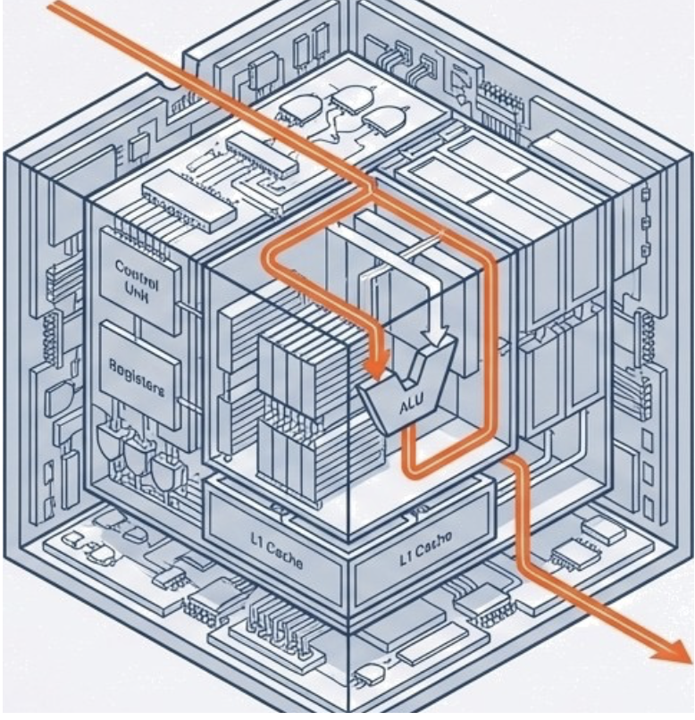
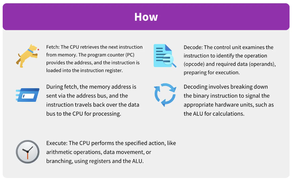
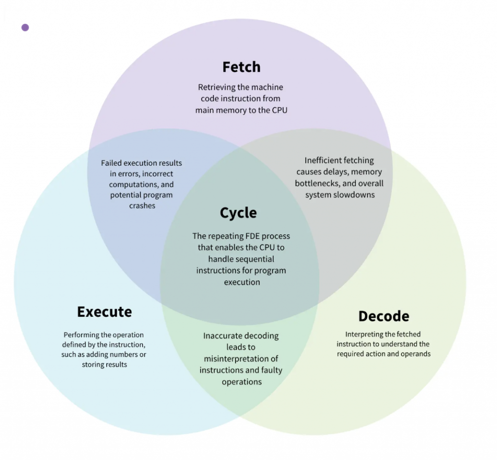
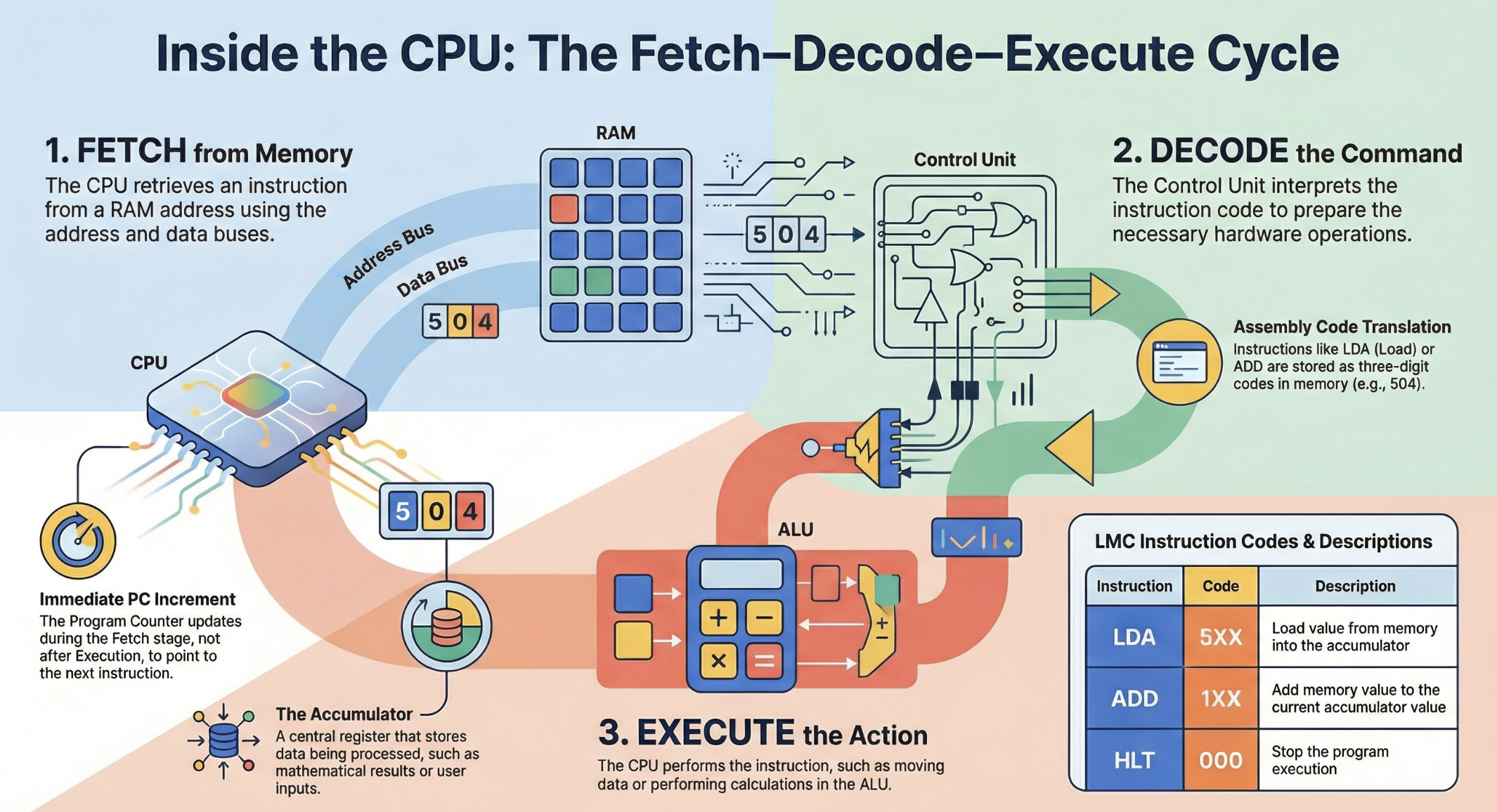
You can think of the FDE cycle as a chef in a kitchen. The Fetch stage is the chef grabbing a recipe from a book (RAM). Decoding is the chef reading and understanding the steps and gathering the necessary tools. Executing is the actual act of cooking the meal using the stove and pans (ALU and Registers). Pipelining is like having an assistant who starts prepping the next recipe as soon as the chef moves a dish to the oven, ensuring the kitchen never stops moving.

Instruction is retrieved
The Program Counter (PC) holds the address of the next instruction
The instruction is fetched from main memory (RAM)
The PC is incremented to point to the next instruction
Key components involved:
PC, MAR, MDR, RAM
Instruction is interpreted
The Control Unit (CU) decodes the instruction
It determines:
What operation is required
Which data is needed
Which components must be activated
Key components involved:
Control Unit, Instruction Register
Instruction is carried out
The instruction is executed by:
ALU (for calculations & logic), or
Other components (memory, I/O)
Results may be stored in registers or memory
Key components involved:
ALU, Registers, Memory
After execution:
The CPU returns to FETCH
This cycle repeats millions or billions of times per second
Use the mark allocation to judge how much detail to include. Questions on the fetch–decode–execute cycle often require a description of the stages alone, rather than an in-depth discussion of registers and buses.
Always mention register names to gain full marks.
P–M–M–I
PC
MAR
MDR
IR
